
Our broad experience in offering demanding PCB design with one or more insulating layers containing signal trace with an exact power and ground for the layout has made us one of the kingpins in providing PCB manufacturing and design services. With our resource efficiency and high quality assurance, we tender quick turn PCB design with reduced fabrication cycles in the designing operations. We have adopted multiple design approaches for tradeoffs and accurate simulation to create a best in class PCB design. The pricing plan follows a fair pricing outlay for rendering PCB design and prototyping services to get quality quick turnarounds for our clients on individual basis.
Our core concentration is to get pre-eminent PCB design, especially for SMD PCB design, thermal analysis and die part creations for silicon or ceramic surfaces with proper tactics by using ground panels which are intrinsic to PCB digital/analog environment that can influence the entire layout philosophy for high performance PCB design.

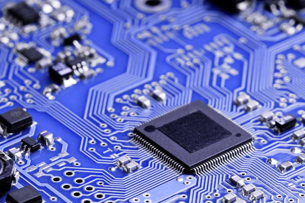
We have enhanced smoothness in fabricating the PCB design by using power integrity, PCB routing , AMS simulation and electrical PCB layouts with over 25 to 25000+ pins with specialization in using Allegro (a Cadence tool) and PADS (an Innerved tool ) to handle your toughest design.
Our varied techniques like full chip electrical verification, turnkey design, custom IC design ,unique design reuse strategies and controlled impedance to deliver ultra high speed design strives to reach out to the requirements of our customers worldwide, MNT Electronics renders services that spans entire execution of custom and heavy-duty design projects.